| CPC H01L 21/31116 (2013.01) [H01L 21/02164 (2013.01); H01L 21/0217 (2013.01)] | 15 Claims |
|
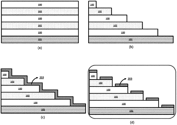
1. A method for fabricating a layer structure having a target topology profile in a step which has a side face and a lateral face, comprising processes of:
(a) depositing a dielectric layer on a preselected area of the substrate under first deposition conditions, wherein the dielectric layer comprises a surface comprising at least a first portion and a second portion, and wherein the first portion is a portion whose resistance to fluorine and/or chlorine radicals under first dry-etching conditions is tuned to have a different resistance to fluorine and/or chlorine radicals under first dry-etching conditions than the second portion; and
(b) exposing the first portion and second portion of the dielectric layer obtained in process (a) to the fluorine and/or chlorine radicals, formed using a remote or indirect plasma, under the first dry-etching conditions, thereby removing at least a part of the first portion of the dielectric layer, thereby forming a layer structure having the target topology profile on the substrate, wherein the target topology profile is either a side face-remaining topology profile or alternatively a lateral face-remaining topology profile,
wherein the first portion comprises an oxide film, and wherein the second portion comprises a silicon nitride film, and
wherein the first portion is deposited under a set of deposition conditions different than the second portion thereby tuning the resistance to fluorine and/or chlorine radicals under first dry-etching conditions of the first portion, wherein the deposition conditions comprise at least one of plasma power, gas selection, gas flow rate, pressure, and temperature in a reaction space.
|