| CPC H01L 21/02247 (2013.01) [H01L 21/02043 (2013.01); H01L 21/02274 (2013.01); H01L 21/28185 (2013.01); H01L 21/28202 (2013.01); H01L 21/67023 (2013.01); H01L 21/67207 (2013.01)] | 10 Claims |
|
1. A method of forming a metal gate structure, the method comprising:
forming a semiconductor structure formed on a substrate, comprising:
forming an interfacial layer on the substrate;
depositing a high-k gate dielectric layer on the interfacial layer;
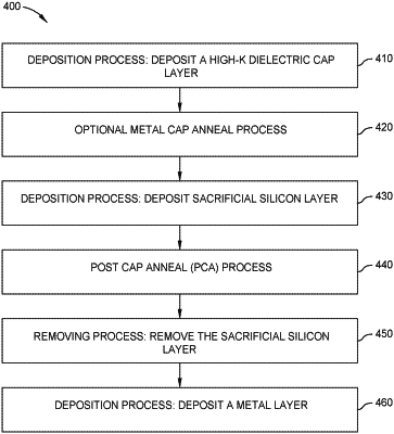
depositing a high-K dielectric cap layer on the semiconductor structure;
performing a metal cap anneal process to harden and densify the high-K dielectric cap layer in a nitrogen (N2) ambient;
depositing a sacrificial silicon cap layer on and in contact with the high-K dielectric cap layer;
performing a post cap anneal process layer in a nitrogen (N2) ambient to harden and densify the deposited high-K dielectric cap layer and the sacrificial silicon cap layer;
removing the sacrificial silicon cap layer; and
depositing a metal layer.
|