| CPC G11C 29/32 (2013.01) [G11C 7/1039 (2013.01); G11C 29/1201 (2013.01); G11C 29/12015 (2013.01); G11C 29/36 (2013.01); G11C 29/42 (2013.01); G01R 31/3172 (2013.01); G01R 31/31723 (2013.01); G01R 31/3177 (2013.01); G01R 31/3185 (2013.01); G01R 31/318536 (2013.01); G01R 31/318541 (2013.01); G01R 31/318544 (2013.01); G01R 31/318547 (2013.01); G01R 31/318566 (2013.01); G01R 31/3187 (2013.01); G06F 11/27 (2013.01); G11C 7/1051 (2013.01); G11C 7/22 (2013.01); G11C 11/4082 (2013.01); G11C 2029/3202 (2013.01)] | 5 Claims |
|
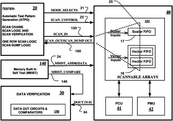
4. An integrated circuit (IC) comprising:
an input buffer enabled to load data during a first part of a clock period;
an array of storage elements, coupled to the input buffer, enabled to load data from the input buffer to a selected row in the array of storage elements in parallel during a second part of the clock period;
an output multiplexor, coupled to the array of storage elements, enabled to output data from a chosen row in the array of storage elements in parallel on a multi-line output data path;
a scan input for a scan chain;
an input multiplexor, coupled to the input buffer, a functional data path, the scan input, and a subset of lines of the multi-line output data path, and enabled to select between the functional data path and a set of inputs including the scan input and the subset of lines of the multi-line output data path as an input to the input buffer; and
a scan output for the scan chain coupled to a line of the output data path.
|