| CPC G11C 13/0069 (2013.01) [G11C 13/003 (2013.01); G11C 13/0038 (2013.01); G11C 13/0026 (2013.01)] | 13 Claims |

|
1. An integrated circuit (IC) device comprising:
an input/output (I/O) pad configured to conduct voltage from a supply voltage; and
a memory circuit including:
an array of non-volatile memory (NVM) cells including rows and columns of memory cells, a particular memory cell is accessed using a word line of a selected row, and a bit line and a source line of a selected column;
an internal supply voltage with a current profile that is not measurable outside the integrated circuit device or the memory circuit;
an isolation circuit controlled by a write type indicator, wherein, when the write type indicator indicates a hidden write operation, the isolation circuit isolates the internal supply voltage from the supply voltage, and the internal supply voltage is selected by the isolation circuit to perform the hidden write operation along a bit line in a selected column of the array of NVM cells;
source line driver circuits; and
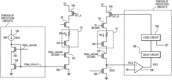
protection circuits, each of the protection circuits are coupled to a respective one of the source line driver circuits, wherein a portion of the respective one of the source line driver circuits is used as part of a cascode current mirror in the protection circuit.
|