| CPC G09G 3/3677 (2013.01) [G09G 3/2096 (2013.01); G09G 3/3225 (2013.01); G09G 3/3266 (2013.01); G09G 3/3275 (2013.01); G09G 3/3648 (2013.01); G09G 3/3688 (2013.01); G09G 2300/0408 (2013.01); G09G 2300/0426 (2013.01); G09G 2300/0465 (2013.01); G09G 2310/0232 (2013.01); H10K 59/131 (2023.02)] | 20 Claims |
|
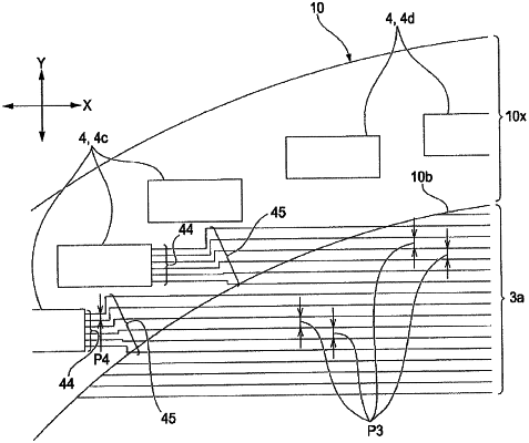
1. An electro-optical device comprising:
a substrate;
gate lines extending in a first direction on the substrate;
a pixel area in which pixel electrodes are disposed;
an outer peripheral edge of the pixel area having a curved portion or a bent portion;
a first circuit block and a second circuit block which are arranged along the curved portion or the bent portion of the outer peripheral edge;
a first gate line included in the gate lines and connected to the first circuit block via a first relay line and a first output line, the first output line extending from the first circuit block, the first relay line connecting an end of the first gate line with an end of the first output line; and
a second gate line included in the gate lines and connected to the second circuit block via a second relay line and a second output line, the second output line extending from the second circuit block, the second relay line connecting an end of the second gate line with an end of the second output line,
wherein a second direction from the end of the first output line to the end of the first gate line is opposite to a third direction from the end of the second output line to the end of the second gate line,
wherein the second direction is orthogonal to the first direction,
wherein the third direction is orthogonal to the first direction.
|