| CPC G06T 7/0008 (2013.01) [G01N 21/9501 (2013.01); G01N 2021/8887 (2013.01); G06T 2207/20081 (2013.01); G06T 2207/30148 (2013.01)] | 20 Claims |
|
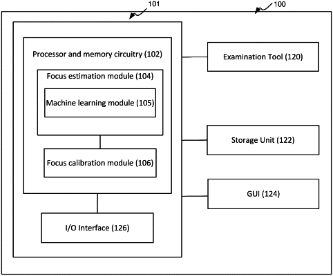
1. A computerized system of runtime defect examination on a semiconductor specimen, the system comprising:
a processing and memory circuitry (PMC),
wherein the PMC is configured to perform a method comprising the steps of:
obtaining, by the PMC, a first image representative of at least part of the semiconductor specimen, wherein the first image is acquired by an examination tool configured with a first focus plane;
estimating, by the PMC, using a machine learning (ML) model, whether the first image is in focus, wherein the ML model is previously trained for classifying images into focused images and defocused images;
upon an estimation that the first image is out of focus, performing, by the PMC, focus calibration on the examination tool so as to select a second focus plane associated with an optimal focus score; and
obtaining, by the PMC, a second image acquired by the examination tool configured with the second focus plane, and estimating, by the PMC, using the ML model, whether the second image is in focus, wherein the second image, upon being estimated as being in focus, is used for defect examination on the semiconductor specimen.
|