US 11,960,719 B2
Semiconductor storage device with volatile and nonvolatile memories to allocate blocks to a memory and release allocated blocks
Hirokuni Yano, Tokyo (JP); Shinichi Kanno, Tokyo (JP); Toshikatsu Hida, Kawasaki (JP); Hidenori Matsuzaki, Fuchu (JP); Kazuya Kitsunai, Kawasaki (JP); and Shigehiro Asano, Yokosuka (JP)
Assigned to Kioxia Corporation, Minato-ku (JP)
Filed by Kioxia Corporation, Minato-ku (JP)
Filed on Oct. 27, 2022, as Appl. No. 17/974,740.
Application 13/571,034 is a division of application No. 13/271,838, filed on Oct. 12, 2011, abandoned.
Application 17/974,740 is a continuation of application No. 17/083,529, filed on Oct. 29, 2020, granted, now 11,513,682.
Application 17/083,529 is a continuation of application No. 16/364,280, filed on Mar. 26, 2019, granted, now 10,845,992, issued on Nov. 24, 2020.
Application 16/364,280 is a continuation of application No. 15/617,220, filed on Jun. 8, 2017, granted, now 10,248,317, issued on Apr. 2, 2019.
Application 15/617,220 is a continuation of application No. 14/822,138, filed on Aug. 10, 2015, granted, now 9,703,486, issued on Jul. 11, 2017.
Application 14/822,138 is a continuation of application No. 14/282,242, filed on May 20, 2014, granted, now 9,134,924, issued on Sep. 15, 2015.
Application 14/282,242 is a continuation of application No. 13/571,034, filed on Aug. 9, 2012, granted, now 8,782,331, issued on Jul. 15, 2014.
Application 13/271,838 is a continuation of application No. 12/552,330, filed on Sep. 2, 2009, granted, now 8,065,470, issued on Nov. 22, 2011.
Application 12/552,330 is a continuation of application No. PCT/JP2008/073950, filed on Dec. 25, 2008.
Claims priority of application No. 2007-339943 (JP), filed on Dec. 28, 2007; and application No. 2008-046227 (JP), filed on Feb. 27, 2008.
Prior Publication US 2023/0042619 A1, Feb. 9, 2023
This patent is subject to a terminal disclaimer.
Int. Cl. G06F 3/06 (2006.01); G06F 12/02 (2006.01); G11C 11/56 (2006.01); G06F 12/0804 (2016.01); G06F 12/0866 (2016.01)
CPC G06F 3/0604 (2013.01) [G06F 3/0616 (2013.01); G06F 3/0631 (2013.01); G06F 3/064 (2013.01); G06F 3/0656 (2013.01); G06F 3/0658 (2013.01); G06F 3/0679 (2013.01); G06F 3/0685 (2013.01); G06F 12/0246 (2013.01); G11C 11/5628 (2013.01); G06F 12/0804 (2013.01); G06F 12/0866 (2013.01); G06F 2212/7201 (2013.01); G06F 2212/7202 (2013.01); G06F 2212/7203 (2013.01); G06F 2212/7209 (2013.01)] 20 Claims
OG exemplary drawing
 
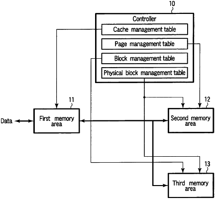
1. A storage device comprising:
a nonvolatile memory including a plurality of blocks, each of the plurality of blocks being a unit of data erasing and configured to store a first data of a first bit; and
a controller configured to:
allocate a first set of the plurality of blocks as a first memory area, the first set of the plurality of blocks each including a first block having a memory cell configured to store a second data of a second bit, the second bit being less than the first bit;
allocate a second set of the plurality of blocks as a second memory area, the second set of the plurality of blocks each including a second block having a memory cell configured to store the first data;
receive data from an external host apparatus;
store the received data into the first block in the first set of the plurality of blocks by a first management unit, the first management unit being less than the unit of data erasing;
copy valid data stored in the first block to the second block by a second management unit, the second management unit being corresponding to the unit of data erasing and being larger than the first management unit; and
release the first block in which no valid data is stored, after copying the valid data stored in the first block,
wherein the first block includes a pseudo block configured to be capable of storing the first data but storing the second data.