| CPC G02F 1/225 (2013.01) [G02B 6/1223 (2013.01); G02B 6/29331 (2013.01); G02F 1/025 (2013.01); G02F 1/292 (2013.01); G02F 1/0151 (2021.01); G02F 2203/10 (2013.01); G02F 2203/20 (2013.01); G02F 2203/24 (2013.01); G02F 2203/50 (2013.01)] | 18 Claims |
|
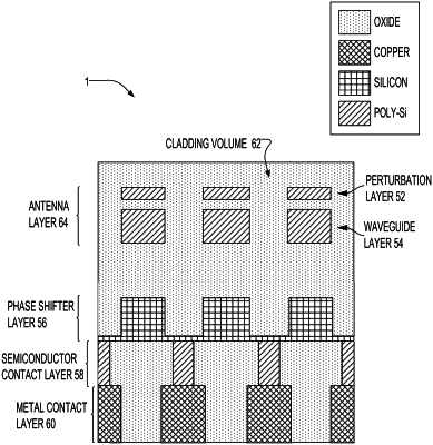
1. An integrated optical device, comprising:
a phase shifter layer comprising an array of phase shifter regions formed from one or more materials including at least a first material, each phase shifter region comprising a first plurality of waveguides and at least one phase shifter for at least a portion of the first plurality of waveguides, wherein each phase shifter region of the array of phase shifter regions is located at a respective position within the array of phase shifter regions;
a splitting network layer, located below the phase shifter layer, comprising a plurality of splitting distribution networks, wherein at least two different splitting distribution networks are configured to couple light provided from or to a different respective initial waveguide to or from a different respective phase shifter region of the array of phase shifter regions; and
an antenna layer, located above the phase shifter layer at a light emitting/receiving portion of the integrated optical device, comprising an array of light-emitting regions formed from one or more materials including at least a second material, each light-emitting region comprising a second plurality of waveguides, wherein each light-emitting region of the array of light-emitting regions is located at a respective position within the array of light-emitting regions, and wherein each light-emitting region of the array of light-emitting regions is configured to emit light received from a phase shifter region located at a position adjacent to a position of the light-emitting region.
|