| CPC G02B 6/4204 (2013.01) [G02B 6/4206 (2013.01); G02B 6/4219 (2013.01); G02B 6/4244 (2013.01); G02B 6/4296 (2013.01); G02B 19/0057 (2013.01); G02B 6/30 (2013.01); G02B 6/4262 (2013.01)] | 14 Claims |
|
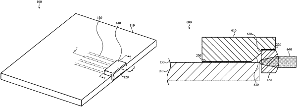
1. A photonics package, comprising:
a substrate comprising:
a connector surface; and
an emitter surface meeting the connector surface at an edge;
a waveguide at least partially within the substrate;
an emitter coupled to the waveguide;
a hanging connector affixed to the connector surface; and
an optical component affixed to the hanging connector; wherein:
the hanging connector comprises:
a base layer;
a top layer; and
a first layer positioned at least partially between the base layer and the top layer; and
a portion of the first layer of the hanging connector forms an angled sidewall and a vertical backstop connecting the top layer of the hanging connector to the base layer of the hanging connector;
the optical component extends along a portion of the emitter surface.
|