| CPC G02B 6/32 (2013.01) | 16 Claims |
|
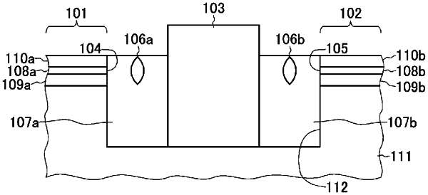
1. An optical connection structure comprising:
a first optical waveguide having a first light incidence/emission end face;
a second optical waveguide having a second light incidence/emission end face facing the first light incidence/emission end face of the first optical waveguide;
an optical element between the first light incidence/emission end face and the second light incidence/emission end face;
a focus lens between the first light incidence/emission end face and the optical element or between the second light incidence/emission end face and the optical element, wherein the focus lens is disposed on an optical axis that connects the first light incidence/emission end face and the second light incidence/emission end face; and
a resin layer having a refractive index different than a refractive index of the focus lens, the resin layer being filled in between the first light incidence/emission end face and the optical element or between the second light incidence/emission end face and the optical element, wherein the focus lens is embedded in the resin layer.
|