| CPC G02B 1/002 (2013.01) [G02B 1/02 (2013.01)] | 18 Claims |
|
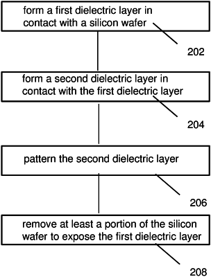
1. A method of fabricating a meta-lens structure, the method comprising:
forming a first dielectric layer in contact with a silicon wafer;
forming a second dielectric layer in contact with the first dielectric layer, a refractive index of the second dielectric layer different from a refractive index of the first dielectric layer;
patterning the second dielectric layer; and
removing at least a portion of the silicon wafer to expose the first dielectric layer,
wherein the silicon wafer is entirely removed;
wherein the method further comprises forming a layer of silicon oxide in contact with the second dielectric layer after the second dielectric layer is patterned and before the silicon wafer is entirely removed; and
wherein the method also comprises bonding a wafer to the silicon oxide layer after the silicon oxide layer is formed, and before the silicon wafer is entirely removed.
|