| CPC G01R 29/10 (2013.01) [H01P 5/107 (2013.01); H01Q 9/0407 (2013.01); H01Q 21/005 (2013.01); H01Q 13/10 (2013.01)] | 12 Claims |
|
1. A microstrip to waveguide transition comprising:
a waveguide module; and
a printed circuit board (PCB),
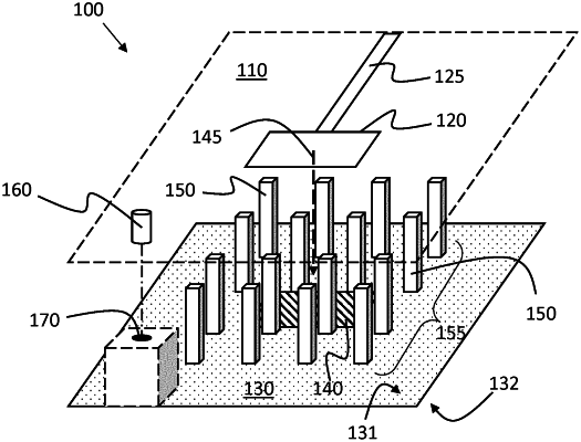
wherein the module is arranged to interface with the PCB, the PCB comprising a patch antenna and a ground plane, the module comprising a waveguide aperture and a repetitive structure, the waveguide aperture arranged extending through the module for attaching a waveguide to an external side of the waveguide module, the repetitive structure comprising a plurality of protruding metal or metallized elements arranged to surround the waveguide aperture on an internal side of the module and to define a passage into the waveguide aperture on the internal side,
wherein the repetitive structure is configured to attenuate electromagnetic signal propagation in a frequency band past the repetitive structure while allowing propagation via the passage,
wherein the repetitive structure and ground plane constitute a gap waveguide structure, and
wherein the repetitive structure is arranged at a distance from the ground plane, where the distance is smaller than a quarter of an operation wavelength of the waveguide module.
|