| CPC G01L 1/12 (2013.01) [H01F 10/3272 (2013.01); H01F 41/302 (2013.01)] | 19 Claims |
|
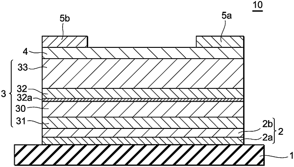
1. A stress sensor comprising:
a stress detection layer including a laminated body including a first ferromagnetic layer, a first non-magnetic layer, a second ferromagnetic layer, and an antiferromagnetic layer stacked one on another, wherein:
the antiferromagnetic layer includes Mn,
a magnetization direction of the second ferromagnetic layer is fixed by an exchange bias caused by an exchange coupling with the antiferromagnetic layer, and
the stress sensor detects a stress by an electric resistance depending upon a relative angle between magnetization directions of the first ferromagnetic layer and the second ferromagnetic layer, the relative angle changing depending upon an externally applied stress,
wherein the electric resistance is detected by a magnitude of a detection current flowing into all layers of the stress detection layer.
|