US 11,959,173 B2
Methods of forming structures, semiconductor processing systems, and semiconductor device structures
Amir Kajbafvala, Chandler, AZ (US); Yanfu Lu, Phoenix, AZ (US); Robinson James, Phoenix, AZ (US); and Caleb Miskin, Mesa, AZ (US)
Assigned to ASM IP Holding B.V., Almere (NL)
Filed by ASM IP Holding B.V., Almere (NL)
Filed on Mar. 17, 2022, as Appl. No. 17/697,079.
Claims priority of provisional application 63/178,749, filed on Apr. 23, 2021.
Claims priority of provisional application 63/162,878, filed on Mar. 18, 2021.
Prior Publication US 2022/0298643 A1, Sep. 22, 2022
Int. Cl. C23C 16/48 (2006.01); C23C 16/24 (2006.01); C23C 16/30 (2006.01); C23C 16/52 (2006.01); G01J 5/00 (2022.01); G01K 7/10 (2006.01); H01L 29/66 (2006.01)
CPC C23C 16/482 (2013.01) [C23C 16/24 (2013.01); C23C 16/30 (2013.01); C23C 16/52 (2013.01); G01J 5/0007 (2013.01); G01K 7/10 (2013.01); H01L 29/66742 (2013.01); H01L 29/66795 (2013.01)] 18 Claims
OG exemplary drawing
 
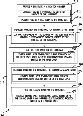
1. A method of forming a structure, comprising:
providing a substrate in a reaction chamber;
forming a first layer overlaying the substrate;
forming a second layer onto the first layer;
wherein temperature of the first layer is controlled during forming the first layer using infrared electromagnetic radiation emitted by the first layer; and
wherein temperature of the second layer is controlled during forming the second layer using infrared electromagnetic radiation emitted by the second layer.