| CPC C23C 16/16 (2013.01) [C23C 16/0218 (2013.01); C23C 16/0245 (2013.01); C23C 16/18 (2013.01); C23C 16/4554 (2013.01); C23C 16/45542 (2013.01); C23C 16/50 (2013.01); H01L 21/02068 (2013.01); H01L 21/02074 (2013.01); H01L 21/2855 (2013.01); H01L 21/28556 (2013.01); H01L 21/28562 (2013.01); H01L 21/324 (2013.01); H01L 21/76849 (2013.01); H01L 21/7685 (2013.01); H01L 21/76862 (2013.01); H01L 21/76883 (2013.01)] | 20 Claims |
|
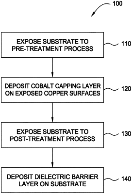
1. A method for capping a copper surface on a substrate, comprising:
positioning a substrate within a processing chamber, wherein the substrate comprises a contaminated copper surface and a dielectric surface;
exposing the contaminated copper surface to a reducing agent while forming a metallic copper surface during a pre-treatment process;
selectively forming a cobalt capping layer on the metallic copper surface while leaving exposed the dielectric surface, comprising:
exposing the substrate to a cobalt precursor gas to form a sublayer of the cobalt capping layer during a vapor deposition process;
exposing the sublayer of the cobalt capping layer to a plasma during a post-treatment process; and
repeating the vapor deposition process and the post-treatment process a plurality of times to deposit additional sublayers to form the cobalt capping layer; and
depositing a dielectric layer on the cobalt capping layer and the dielectric surface.
|