| CPC H01L 29/0684 (2013.01) [H01L 29/0865 (2013.01); H01L 29/0878 (2013.01); H01L 29/0882 (2013.01); H01L 29/1095 (2013.01); H01L 29/1608 (2013.01); H01L 29/7802 (2013.01); H01L 29/7827 (2013.01)] | 13 Claims |

|
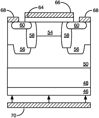
[ 26. A transistor device comprising:
a substrate;
a drift layer on the substrate;
a spreading layer on the drift layer, the spreading layer comprising a first doping type;
a pair of junction implants that are provided to a first depth in the spreading layer, wherein each of the junction implants in the pair of junction implants comprises:
a well region with a second doping type that is opposite the first doping type; and
a base region with the second doping type;
wherein the well region is provided to the first depth in the spreading layer, and the base region is provided to a second depth in the spreading layer that is less than the first depth; and
a JFET region that is provided to a third depth in the spreading layer that is less than the first depth and less than the second depth;
wherein a thickness of the spreading layer is in a range from 1.0 to 2.5 microns and is provided at a fourth depth that is greater than the first depth, and
wherein a thickness of the JFET region is in a range from 0.75 to 1.5 microns.]
|