| CPC H01L 23/49541 (2013.01) [H01L 21/4853 (2013.01); H01L 21/4882 (2013.01); H01L 21/561 (2013.01); H01L 21/565 (2013.01); H01L 23/293 (2013.01); H01L 23/3142 (2013.01); H01L 23/3157 (2013.01); H01L 23/373 (2013.01); H01L 23/3731 (2013.01); H01L 23/4334 (2013.01); H01L 23/49503 (2013.01); H01L 23/49555 (2013.01); H01L 23/49568 (2013.01); H01L 24/73 (2013.01); H01L 27/0211 (2013.01); H01L 2224/32245 (2013.01); H01L 2224/48091 (2013.01); H01L 2224/48137 (2013.01); H01L 2224/48247 (2013.01); H01L 2224/73265 (2013.01); H01L 2924/13055 (2013.01); H01L 2924/181 (2013.01)] | 65 Claims |

|
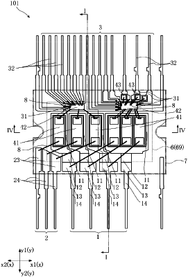
1. A semiconductor device, comprising:
a first island part;
a first semiconductor chip mounted on the first island part;
a second island part;
a second semiconductor chip mounted on the second island part;
a third island part;
a third semiconductor chip mounted on the third island part;
a fourth island part;
a fourth semiconductor chip mounted on the fourth island part;
a fifth semiconductor chip mounted on the fourth island part;
a sixth semiconductor chip mounted on the fourth island part;
a fifth island part;
a first driving semiconductor chip mounted on the fifth island part and connected to each of the first to third semiconductor chips;
a sixth island part;
a second driving semiconductor chip mounted on the sixth island part and connected to each of the fourth to sixth semiconductor chips;
a first lead terminal connected to the first semiconductor chip by a first wire;
a second lead terminal connected to the second semiconductor chip by a second wire;
a third lead terminal connected to the third semiconductor chip by a third wire;
a fourth lead terminal connected to the fourth semiconductor chip by a fourth wire;
a fifth lead terminal connected to the fifth semiconductor chip by a fifth wire;
a sixth lead terminal connected to the sixth semiconductor chip by a sixth wire; and
a seventh lead terminal extending from the fourth island part,
wherein the first to sixth semiconductor chips are arranged in a first direction,
the first lead terminal is longer than the second lead terminal in a second direction perpendicular to the first direction, and
the second lead terminal is longer than the third lead terminal in the second direction [ , and
wherein the first to sixth wires are directly connected to the first to sixth lead terminals, respectively, and the first to sixth wires are electrically connected only between the first to sixth lead terminals and the first to sixth semiconductor chips respectively] .
|