| CPC H10N 60/0156 (2023.02) [H01L 21/76891 (2013.01); H01L 23/5223 (2013.01); H01L 23/5226 (2013.01); H01L 23/5227 (2013.01); H01L 23/528 (2013.01); H01L 23/53257 (2013.01); H01L 23/53285 (2013.01); H10N 60/85 (2023.02); H10N 69/00 (2023.02)] | 20 Claims |

|
1. An integrated circuit structure, comprising:
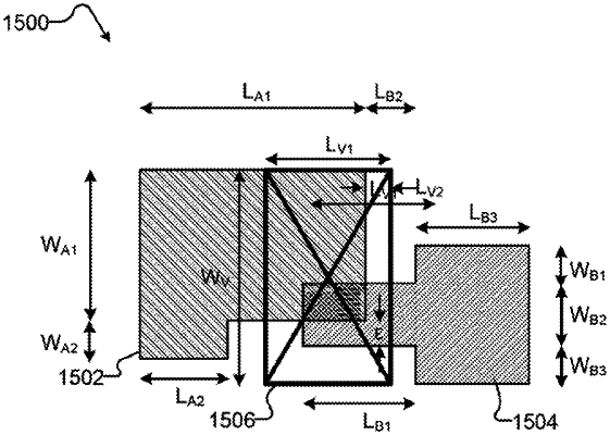
a first wiring layer that comprises an electrically conductive material and which resides in a first plane, the first wiring layer comprising a first mark, the first mark having a first set of nominal dimensions and a first resistance specified at least in part by the first set of nominal dimensions;
a second wiring layer that comprises an electrically conductive material and which resides in a second plane which at least partially overlies the first plane, the second wiring layer comprising a second mark, the second mark having second set of nominal dimensions and a second resistance specified at least in part by the second set of nominal dimensions, the second mark having a nominal position along at least one coordinate axis with respect to the first mark; and
a first stud via that comprises an electrically conductive material and which resides in between the first and the second planes, the first stud via having a third set of nominal dimensions and a third resistance specified at least in part by the third set of nominal dimensions, the first stud via which provides a signal path between the first mark and the second mark, the second mark which overlaps the stud via in a first resistive overlap region defined by an orthogonal projection of the second mark on the stud via, the first resistance overlap region having a resistance that is larger than a cumulative resistance of the first mark, the second mark and the stud via at least at temperatures above a critical temperature.
|