| CPC H10K 85/633 (2023.02) [H10K 85/6572 (2023.02); H10K 50/115 (2023.02); H10K 50/15 (2023.02); H10K 50/16 (2023.02); H10K 50/17 (2023.02); H10K 71/00 (2023.02); H10K 71/12 (2023.02); H10K 2102/331 (2023.02); H10K 2102/351 (2023.02)] | 26 Claims |

|
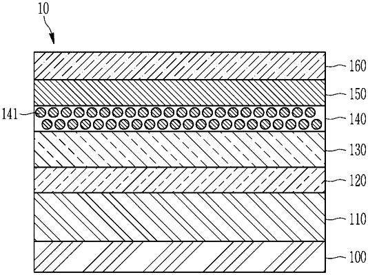
1. An electroluminescent device, comprising
a first electrode and a second electrode facing each other;
an emission layer disposed between the first electrode and the second electrode and comprising
a plurality of quantum dots, and
a first hole transporting material comprising an unsubstituted C4 to C20 alkyl group attached to a backbone structure, wherein the first hole transporting material is a non-polymeric compound;
a hole transport layer disposed between the emission layer and the first electrode and comprising a second hole transporting material;
an electron transport layer disposed between the emission layer and the second electrode; and
wherein the first hole transporting material is a fluorenyl amine compound and the unsubstituted C4 to C20 alkyl group is attached to a fluorenyl group of the fluorenyl amine compound.
|