| CPC H10K 71/00 (2023.02) [H10K 50/822 (2023.02); H10K 59/12 (2023.02); H10K 59/1201 (2023.02); H10K 2102/351 (2023.02)] | 7 Claims |

|
1. A method of manufacturing a display device, comprising the steps of:
S1: providing a substrate, and sequentially forming an array circuit, an anode layer and a light-emitting layer on the substrate;
S2: forming a first cathode layer upon the light-emitting layer with cathode material processed by evaporation coating;
S3: forming a mounting hole in a non-display area by etching;
S4: using a mask assembly to shield an area where the mounting hole is located, and forming a second cathode layer with cathode material processed by evaporation coating;
wherein the second cathode layer covers both a transitional-display area and a display area, and the first cathode layer produced in the step S2 and the second cathode layer produced in the step S4 together constitute a cathode layer of the display device;
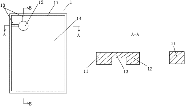
wherein the mask assembly used in the step S4 comprises:
a mask frame, having an open area and configured to be supported on a surface of the substrate during evaporation coating in the step S4;
a plurality of island shelters, located in the open area and configured to be in contact with the surface of the substrate through the mounting hole during evaporation coating in the step S4; and
at least one connection bridge, configured to be spaced apart from and suspended above the surface of the substrate to form a gap between the at least one connection bridge and the surface of the substrate during evaporation coating in the step S4,
wherein at least one of the plurality of island shelters is connected to the mask frame or a neighboring island shelter of the plurality of the island shelters via the at least one connection bridge.
|