| CPC H10K 59/40 (2023.02) [H10K 59/8731 (2023.02); H10K 71/60 (2023.02)] | 20 Claims |

|
1. A touch display panel, comprising:
a drive back plate;
a light-emitting device, disposed on the drive back plate;
an encapsulation layer, disposed on a side of the light-emitting device distal from the drive back plate; and
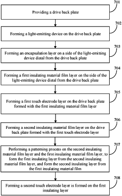
a touch layer, disposed on a side of the encapsulation layer distal from the light-emitting device, wherein the touch layer comprises a first touch electrode layer and a second touch electrode layer laminated in sequence, and the touch layer further comprises a touch insulating layer disposed between the first touch electrode layer and the second touch electrode layer and/or between the first touch electrode layer and the encapsulation layer, wherein a smallest space between a boundary of the drive back plate and at least portion of a boundary, most proximal to the boundary of the drive back plate, of the touch insulating layer is smaller than a smallest space between the boundary of the drive back plate and a boundary, most proximal to the boundary of the drive back plate, of the encapsulation layer.
|