| CPC H10K 59/131 (2023.02) [H10K 59/1201 (2023.02); H10K 2102/341 (2023.02)] | 17 Claims |

|
1. A display device having: a display area in which there is provided a pixel circuit; and a frame area in which there is provided a plurality of drivers, the display device comprising:
a plurality of control lines;
a plurality of power supply lines parallel to the plurality of control lines;
a plurality of data signal lines crossing the plurality of control lines;
an oxide semiconductor layer;
a first metal layer containing the plurality of control lines therein;
a gate insulation film;
a first inorganic insulation film overlying the gate insulation film;
a second metal layer overlying the first inorganic insulation film and containing the plurality of power supply lines therein;
a second inorganic insulation film overlying the second metal layer; and
a third metal layer overlying the second inorganic insulation film and containing the plurality of data signal lines therein, wherein
the gate insulation film has a top face in contact with either one of the oxide semiconductor layer and the first metal layer and a bottom face in contact with another one of the oxide semiconductor layer and the first metal layer,
each of the plurality of control lines is electrically connected to an associated one of the plurality of drivers via the third metal layer,
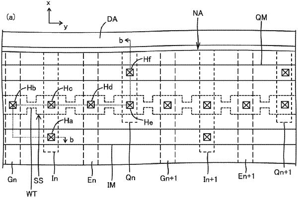
the oxide semiconductor layer, in a plan view, contains therein semiconductor lines formed as isolated regions between the plurality of drivers and the display area, and
the semiconductor lines cross the plurality of control lines and the plurality of power supply lines, are in contact with the plurality of control lines via at least one opening in the gate insulation film, are in contact with the plurality of power supply lines via at least one opening in the first inorganic insulation film, and have a plurality of narrowed portions, such that thicker and thinner regions exist along the same line.
|