| CPC H10K 59/131 (2023.02) [G09G 3/006 (2013.01); H10K 50/844 (2023.02)] | 20 Claims |

|
1. A display panel, comprising:
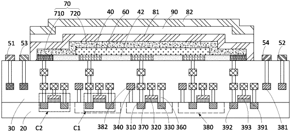
a silicon-based substrate, comprising a display region and a peripheral region surrounding the display region;
a driving layer, formed in the silicon-based substrate, and comprising a plurality of first transistors located in the display region;
a first electrode layer, disposed on a side of the driving layer away from the silicon-based substrate, and comprising a plurality of first electrodes located in the display region, and each of the first electrodes is electrically connected to each of the first transistors;
an organic light emitting layer, disposed on a side of the first electrode layer away from the driving layer;
a second electrode layer, disposed on a side of the organic light emitting layer away from the driving layer, and comprising a second electrode located in the display region and an electrode ring located in the peripheral region, the electrode ring being configured to surround the second electrode and being connected to the second electrode; and
a plurality of pads, located in the peripheral region at least one side of the display region, the plurality of pads comprising a display signal access pad and a test signal access pad, and the test signal access pad being located at both sides of the display signal access pad;
wherein the display signal access pad is configured to access the display signal during a display phase, and the test signal access pad is configured to access the test signal during a test phase, the test signal access pad at least comprises a first group of test phase access pads, and the first group of test phase access pads comprises a first pad and a second pad, the first pad is electrically connected with the electrode ring, and the second pad is electrically connected with the silicon-based substrate.
|