| CPC H10K 59/122 (2023.02) [H10K 59/1201 (2023.02); H10K 59/8792 (2023.02)] | 20 Claims |

|
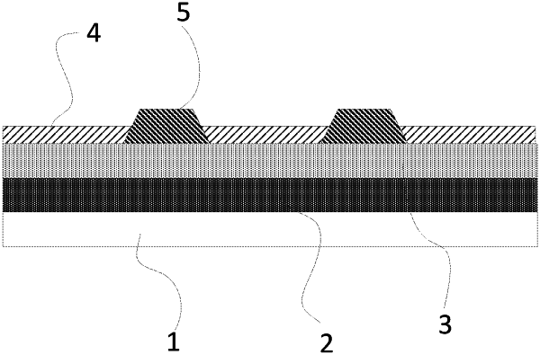
1. An array substrate, comprising:
a base substrate;
a driving circuit structure on the base substrate,
a planarization layer and a plurality of electrode structures successively located on a side, facing away from the base substrate, of the driving circuit structure;
insulation structures in gap areas between adjacent electrode structures among the plurality of electrode structures; wherein a thickness of the insulation structures is not smaller than a thickness of the electrode structures; and
pixel defining structures on a side, facing away from the base substrate, of the insulation structures; wherein an orthographic projection of the pixel defining structures on the base substrate at least completely covers the insulation structures;
wherein hydrophilicity of the planarization layer, hydrophilicity of the insulation structures and hydrophilicity of the pixel defining structures decrease successively.
|