US 11,956,997 B2
Display device
Se Wan Son, Hwaseong-si (KR); Nak Cho Choi, Yongin-si (KR); Moo Soon Ko, Seoul (KR); Dong Hyun Son, Seoul (KR); Sang Hoon Oh, Seoul (KR); Jin Goo Jung, Seongnam-si (KR); Kyung Hyun Choi, Seoul (KR); Hae-Yeon Lee, Hwaseong-si (KR); and Seong Min Cho, Seongnam-si (KR)
Assigned to Samsung Display Co., Ltd., Gyeonggi-Do Yongin-Si (KR)
Filed by Samsung Display Co., Ltd., Yongin-Si (KR)
Filed on Aug. 23, 2021, as Appl. No. 17/445,718.
Claims priority of application No. 10-2020-0137710 (KR), filed on Oct. 22, 2020.
Prior Publication US 2022/0130915 A1, Apr. 28, 2022
Int. Cl. H10K 59/121 (2023.01); H10K 50/86 (2023.01); H10K 59/122 (2023.01); H10K 59/38 (2023.01); H10K 59/40 (2023.01); H10K 59/65 (2023.01)
CPC H10K 59/121 (2023.02) [H10K 50/865 (2023.02); H10K 59/122 (2023.02); H10K 59/38 (2023.02); H10K 59/40 (2023.02); H10K 59/65 (2023.02)] 20 Claims
OG exemplary drawing
 
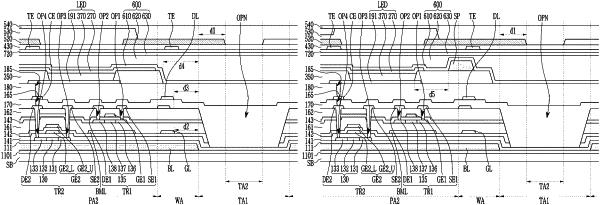
1. A display device comprising:
a substrate including a display area and a transmission area;
a metal blocking layer disposed in the display area of the substrate;
an inorganic insulating layer disposed on the metal blocking film;
a transistor disposed on the inorganic insulating layer;
an emission layer connected to the transistor; and
a light blocking layer and a color filter disposed on the emission layer of the display area,
wherein the edge of the light blocking layer is protruded toward the transmission area more than the edge of the metal blocking layer.