| CPC H10K 50/86 (2023.02) [H10K 50/844 (2023.02); H10K 50/865 (2023.02); H10K 59/12 (2023.02); H10K 59/40 (2023.02); H10K 77/10 (2023.02); G02F 1/133305 (2013.01); G02F 1/133331 (2021.01); G02F 1/133528 (2013.01); G06F 1/1641 (2013.01); G06F 1/1652 (2013.01); G09F 9/301 (2013.01); G09G 2380/02 (2013.01); H01L 27/14678 (2013.01); H10K 50/8426 (2023.02); H10K 50/868 (2023.02); H10K 59/126 (2023.02); H10K 77/111 (2023.02); H10K 2102/311 (2023.02); H10K 2102/351 (2023.02)] | 10 Claims |

|
1. An OLED display panel, comprising:
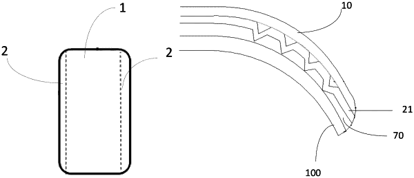
a flat display area and an edge curved-surface display area; wherein the edge curved-surface display area is provided with an optical film layer, and the optical film layer is configured to reduce a light intensity of emergent light with a preset color in the edge curved-surface display area;
a light-emitting unit; and
an encapsulation layer,
wherein the encapsulation layer is disposed on a side of the light-emitting unit close to a light-emitting surface of the OLED display panel and the optical film layer is disposed on a side of the encapsulation layer away from the light-emitting unit, and
wherein the optical film layer comprises a reflection enhancing film; subsequent to an entrance of an incident light into the reflection enhancing film, a propagation distance d of the incident light in the reflection enhancing film satisfies a following formula: 2nd=(2k+1)λ/2, to increase a reflectivity of light with a wavelength of λ, where k=0, 1, 2 . . . , n is a refractive index of the reflection enhancing film.
|