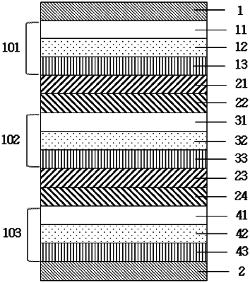
| CPC H10K 50/19 (2023.02) [H10K 50/11 (2023.02); H10K 85/342 (2023.02); H10K 85/40 (2023.02); H10K 85/60 (2023.02); H10K 85/615 (2023.02); H10K 85/622 (2023.02); H10K 85/626 (2023.02); H10K 85/633 (2023.02); H10K 85/636 (2023.02); H10K 85/654 (2023.02); H10K 85/6572 (2023.02); H10K 85/6574 (2023.02); H10K 2102/351 (2023.02)] | 12 Claims |

|
1. An organic light emitting device comprising:
an anode;
a cathode provided to face the anode;
two or more light emitting layers provided between the anode and the cathode and each having a maximum light emission peak at a wavelength of 500 nm or less; and
a light emitting layer having a maximum light emission peak at a wavelength of more than 500 nm provided between the two or more light emitting layers each having a maximum light emission peak at a wavelength of 500 nm or less,
wherein a distance from the anode to the light emitting layer having a maximum light emission peak at a wavelength of 500 nm or less, which is the most adjacent to the anode, is 100 nm to 200 nm,
a distance from the anode to the light emitting layer having a maximum light emission peak at a wavelength of 500 nm or less, which is the most adjacent to the cathode, is 3 times to 4 times the distance from the anode to the light emitting layer having a maximum light emission peak at a wavelength of 500 nm or less, which is the most adjacent to the anode,
an N-type charge generation layer and a P-type charge generation layer are provided between each of the light emitting layers each having a maximum light emission peak at a wavelength of 500 nm or less and the light emitting layer having a maximum light emission peak at a wavelength of more than 500 nm, and
the N-type charge generation layer comprises an alkali metal, and the P-type charge generation layer comprises a material having an electron affinity of 4.8 eV or more,
wherein the distance from the anode to the light emitting layer having a maximum light emission peak at a wavelength of 500 nm or less, which is the most adjacent to the anode means the distance from an interface between the anode and a layer which is adjacent to a side of the anode, which faces the cathode to an interface between the light emitting layer having a maximum light emission peak at 500 nm or less, which is the most adjacent to the anode, and the layer which is adjacent to the side of the anode, which faces the cathode, and
wherein the distance from the anode to the light emitting layer having a maximum light emission peak at a wavelength of 500 nm or less, which is the most adjacent to the cathode means the distance from the interface between the anode and the layer which is adjacent to the side of the anode, which faces the cathode to an interface between the light emitting layer having a maximum light emission peak at a wavelength of 500 nm or less, which is the most adjacent to the cathode, and a layer which is adjacent to a side of the light emitting layer having a maximum light emission peak at a wavelength of 500 nm or less, which is the most adjacent to the cathode, which faces the anode.
|