| CPC H10B 99/00 (2023.02) [C23C 16/0281 (2013.01); C23C 16/047 (2013.01); C23C 14/221 (2013.01); C23C 14/225 (2013.01); C23C 16/0209 (2013.01); C23C 16/45525 (2013.01); H01L 21/28562 (2013.01)] | 13 Claims |

|
1. A method of forming multi-level device contact, comprising:
providing a substrate, the substrate defining a plane of the substrate and having an array of spacer features, disposed over an array of active device features, arranged in a first level; and
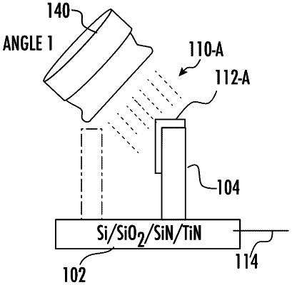
directing a reactive beam to the array of spacer features, the reactive beam defining a non-zero angle of incidence with respect to a perpendicular to the plane of the substrate, wherein a seed layer is deposited on a first portion of the array of spacer features, and is not deposited on a second portion of the array of spacer features,
wherein the reactive beam comprises a metallic species, and wherein the seed layer forms an array of staggered contacts, having an S-shape.
|