| CPC H10B 63/30 (2023.02) [H10B 61/22 (2023.02); H10B 63/80 (2023.02); H10N 50/01 (2023.02); H10N 70/011 (2023.02)] | 18 Claims |

|
1. A memory fabrication method, comprising:
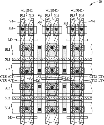
forming a plurality of gate electrode lines to respectively form a plurality of gates of a plurality of data storage cells, wherein the plurality of data storage cells are arranged in an array; and
forming a plurality of conductive lines, wherein each of the plurality of conductive lines is coupled to two of the plurality of gate electrode lines, and each of the plurality of conductive lines at least partially overlaps the two gate electrode lines of the plurality of gate electrode lines,
wherein the plurality of conductive lines comprise a plurality of first conductive lines and a plurality of second conductive lines, the plurality of first conductive lines are perpendicular to the plurality of second conductive lines, one of the plurality of first conductive lines overlapping one of the plurality of second conductive lines are staggered and non-aligned with another of the plurality of first conductive lines overlapping another of the plurality of second conductive lines.
|