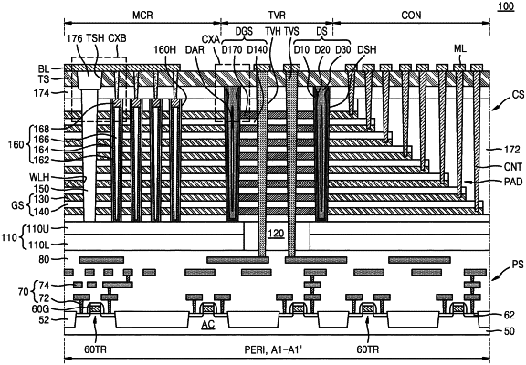
| CPC H10B 43/40 (2023.02) [H10B 41/10 (2023.02); H10B 41/27 (2023.02); H10B 41/35 (2023.02); H10B 41/40 (2023.02); H10B 43/10 (2023.02); H10B 43/27 (2023.02); H10B 43/35 (2023.02)] | 20 Claims |

|
1. An integrated circuit device, comprising:
a peripheral circuit structure arranged on a substrate;
a gate stack arranged on the peripheral circuit structure,
wherein the gate stack comprises a plurality of gate electrodes spaced apart from each other in a first direction substantially perpendicular to a top surface of the substrate;
a dam structure formed in a dam opening portion that passes through the gate stack,
wherein the dam structure comprises:
an insulation spacer arranged on an inner wall of the dam opening portion and comprising a pair of sloped sidewalls at an upper side of the dam opening portion; and
a buried layer filling an inside of the dam opening portion and comprising aft one air space completely surrounded by the buried layer and extending through the gate stack in the first direction,
wherein the one air space is adjacent to a gate electrode of the plurality of gate electrodes that is closer to a top of the gate stack than to a bottom of the gate stack, and is adjacent to another gate electrode of the plurality of gate electrodes that is closer to the bottom of the gate stack than to the top of the gate stack;
a mold gate stack surrounded by the dam structure and comprising a plurality of mold layers spaced apart from each other in the first direction;
a plurality of conductive lines arranged on the gate stack, the mold gate stack, and the dam structure; and
a plurality of through electrodes connected to the plurality of conductive lines, extending to the peripheral circuit structure through the mold gate stack, and surrounded by the dam structure.
|