| CPC H10B 43/35 (2023.02) [H10B 41/27 (2023.02); H10B 41/35 (2023.02); H10B 41/41 (2023.02); H10B 43/27 (2023.02); H10B 43/40 (2023.02)] | 17 Claims |

|
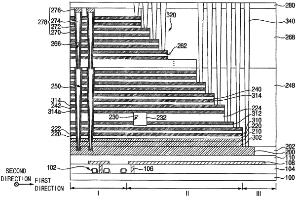
1. A memory device, comprising:
a substrate;
a first insulation layer on the substrate:
a ground selection line on the first insulation layer, a cutting portion cutting the ground selection line;
an uppermost first insulation layer and a first word line stacked immediately above the ground selection line; and
second insulation layers and second word lines alternately stacked on the first word line,
wherein:
the first word line includes a first portion laterally offset from the cutting portion and a second portion overlying the cutting portion,
the first portion of the first word line has a first thickness,
the second portion of the first word line has a second thickness less than the first thickness,
each of the second word lines has the first thickness,
the cutting portion includes an opening passing through the uppermost first insulation layer, cutting the ground selection line, and extending into a portion of the first insulation layer,
a lower insulation pattern is in the opening, and
the uppermost first insulation layer has a thickness that is about 2 times to about 5 times a thickness of the first insulation layer.
|