| CPC H10B 43/27 (2023.02) [H10B 41/10 (2023.02); H10B 41/27 (2023.02); H10B 43/10 (2023.02)] | 20 Claims |

|
1. A semiconductor memory device comprising:
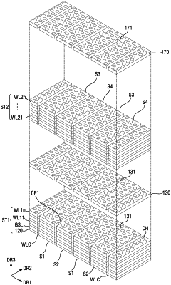
a first stacked structure on a substrate, the first stacked structure including first gate electrodes stacked in a first direction;
a first supporter layer on the first stacked structure, the first supporter layer divided by a first cut pattern;
a second stacked structure on the first supporter layer, the second stacked structure including second gate electrodes stacked in the first direction;
a block cut structure extending in a second direction intersecting the first direction and cutting at least one of the second stacked structure or the first stacked structure;
a second supporter layer on the second stacked structure and divided by a second cut pattern; and
a channel structure including a lower channel structure penetrating the first stacked structure, and an upper channel structure penetrating the first supporter layer and the second stacked structure,
wherein a width of an upper face of the channel structure in a third direction intersecting the second direction is greater than a width of a lower surface of the channel structure in the third direction, a width of an uppermost face of the lower channel structure in the second direction is greater than a width of a lowermost face of the upper channel structure in the second direction,
the first stacked structure includes a first stack and a second stack which are at least partially divided by the block cut structure,
the second stacked structure includes a third stack on the first stack, and a fourth stack on the second stack, the third stack and the fourth stack separated by the block cut structure,
the first supporter layer is on the first stack and the second stack,
the second supporter layer is on the third stack and the fourth stack,
the first cut pattern of the first supporter layer includes a first connection on the block cut structure, the first connection connecting the first supporter layer on the first stack with the second stack,
the second cut pattern of the second supporter layer includes a second connection on the block cut structure, the second connection connecting the second supporter layer on the third stack with the fourth stack, and
a ratio of an area of the first connection to an area of the first supporter layer is different than a ratio of an area of the second connection to an area of the second supporter layer.
|