| CPC H10B 43/27 (2023.02) [H01L 23/5226 (2013.01); H10B 43/10 (2023.02); H10B 43/35 (2023.02); H10B 43/40 (2023.02)] | 28 Claims |

|
1. An electronic device comprising:
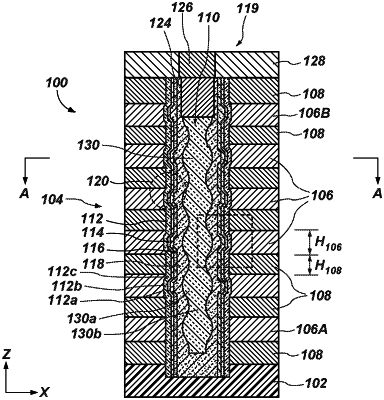
a stack of alternating dielectric materials and conductive materials arranged in tiers, each of the tiers including a dielectric material and a conductive material vertically neighboring the dielectric material;
a pillar region extending vertically through the stack;
an oxide material comprising a single material composition within the pillar region and laterally adjacent to and directly physically contacting the dielectric materials and the conductive materials of the stack; and
a storage node laterally adjacent to and directly physically contacting the oxide material and within the pillar region, a charge confinement region of the storage node in horizontal alignment with the conductive materials of the stack, and a height of the charge confinement region in a vertical direction less than a height of a respective, laterally adjacent conductive material of the stack in the vertical direction.
|