| CPC H10B 41/41 (2023.02) [G11C 16/30 (2013.01); G11C 16/32 (2013.01); G11C 5/14 (2013.01); G11C 11/413 (2013.01)] | 19 Claims |

|
1. A semiconductor integrated circuit comprising:
a first power supply line to which a first voltage is supplied;
a second power supply line to which a second voltage lower than the first voltage is supplied;
a third power supply line to which a third voltage higher than the second voltage is supplied;
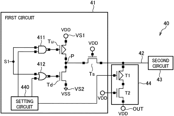
a first circuit that is connected between the first power supply line and the second power supply line, includes a level shift transistor, and is configured to output a signal having an amplitude lower than the first voltage by a threshold voltage of the level shift transistor;
a transmission line through which the signal output from the first circuit propagates;
a second circuit connected the transmission line to receive the signal propagating through the transmission line; and
a third circuit connected between the transmission line and the third power supply line and configured to allow a current to flow from the transmission line when a voltage of the transmission line exceeds a set voltage.
|