| CPC H10B 20/20 (2023.02) [H01L 21/02532 (2013.01); H01L 21/02603 (2013.01); H01L 21/30604 (2013.01); H01L 21/823431 (2013.01); H01L 29/0673 (2013.01); H01L 29/42384 (2013.01); H01L 29/42392 (2013.01); H01L 29/4908 (2013.01); H01L 29/66545 (2013.01); H01L 29/66742 (2013.01); H01L 29/78696 (2013.01); H10B 20/00 (2023.02)] | 20 Claims |

|
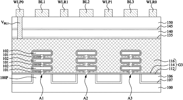
1. A memory device, comprising:
a substrate;
a first transistor and a second transistor over the substrate and electrically connected to each other, wherein each of the first and second transistors comprises:
first semiconductor layers and second semiconductor layers alternately stacked over the substrate;
a gate structure crossing the first semiconductor layers and the second semiconductor layers, wherein in a cross-sectional view where the gate structure crosses the first semiconductor layers and the second semiconductor layers, the first semiconductor layers are in contact with the second semiconductor layers, and a width of the first semiconductor layers is narrower than a width of the second semiconductor layers; and
source/drain structures on opposite sides of the gate structure;
a first word line electrically connected to the gate structure of the first transistor;
a second word line electrically connected to the gate structure of the second transistor; and
a bit line electrically connected to a first one of the source/drain structures of the first transistor.
|