| CPC H10B 12/482 (2023.02) [H01L 23/5283 (2013.01); H01L 23/53295 (2013.01); H10B 12/485 (2023.02); G11C 5/063 (2013.01)] | 13 Claims |

|
1. A method of formation a semiconductor structure, comprising steps of:
providing a substrate, wherein a substrate isolation layer is disposed on a top surface of the substrate, wherein the substrate comprises bit line contact regions and isolation regions, wherein each of the isolation regions is located between adjacent two of the bit line contact regions;
forming a stack of layers on the substrate isolation layer;
forming a first etching window on the stack of layers, and etching the stack of layers and the substrate isolation layer along the first etching window;
removing the stack of layers from a top surface of the substrate isolation layer outside the first etching window;
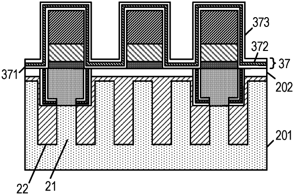
forming a groove along the first etching window in the substrate, wherein a bottom of the groove exposes one of the bit line contact regions and two of the isolation regions adjacent to said one of the bit line contact regions;
forming a contact region isolation layer covering sidewalls of the groove;
forming a bit line contact layer covering a surface of the contact region isolation layer and filling the groove, wherein the bit line contact layer is arranged to be in contact with said one of the bit line contact regions at the bottom of the groove; and
forming a bit line layer on the bit line contact layer.
|