| CPC H10B 12/30 (2023.02) [H10B 12/03 (2023.02); H10B 12/05 (2023.02)] | 13 Claims |

|
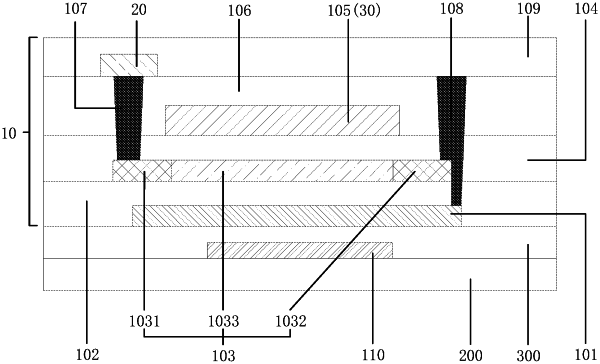
1. A memory, comprising a substrate, and word lines, bit lines and memory cells on one side of the substrate;
each of the memory cells comprises a transistor, and the transistor comprises:
a semiconductor layer comprising a source contact region, a channel region and a drain contact region connected sequentially;
a primary gate electrically connected to one of the word lines;
a source electrically connected to one of the bit lines and the source contact region of the semiconductor layer, respectively;
a drain electrically connected to the drain contact region of the semiconductor layer; and
a secondary gate electrically connected to the drain;
wherein an orthographic projection of the primary gate on the substrate and an orthographic projection of the secondary gate on the substrate are at least partially overlapped with an orthographic projection of the channel region of the semiconductor layer on the substrate, respectively;
the memory cell further comprises a storage structure comprising the secondary gate,
wherein a node capacitors between the secondary gate and the drain being used as a storage capacitor of the memory cell, so that data “1” or “0” is stored in the storage capacitor in a writing state, and whether “1” or “0” being stored is determined according to ON or OFF of the transistor in a reading state,
wherein the storage structure further comprises a first electrode, the storage capacitor being formed between the secondary gate and the first electrode, and
wherein the primary gate is located between the substrate and the semiconductor layer, the secondary gate is located on one side of the semiconductor layer away from the substrate, and the first electrode is located on one side of the secondary gate away from the substrate.
|