| CPC H10B 12/30 (2023.02) [H01L 21/02258 (2013.01); H01L 21/02565 (2013.01); H01L 29/24 (2013.01); H01L 29/66969 (2013.01); H01L 29/78642 (2013.01); H01L 29/7869 (2013.01); H10B 12/036 (2023.02); H10B 12/05 (2023.02); H10B 12/50 (2023.02)] | 11 Claims |

|
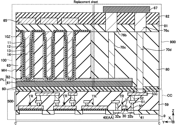
1. A memory device comprising:
a semiconductor substrate;
a circuit provided on a first surface of the semiconductor substrate and including a first contact portion;
an aluminum oxide layer provided above the semiconductor substrate in a first direction perpendicular to the first surface;
a memory cell including a capacitor, the capacitor being provided in the aluminum oxide layer;
a first conductive layer provided between the semiconductor substrate and the aluminum oxide layer in the first direction and electrically connected to the memory cell;
a first insulating layer provided between the first conductive layer and the semiconductor substrate in the first direction;
a second insulating layer adjacent to the aluminum oxide layer in a second direction parallel to the first surface and provided above the semiconductor substrate in the first direction; and
a second contact portion provided in the second insulating layer and above the first contact portion in the first direction to electrically connect the memory cell to the first contact portion,
wherein the capacitor includes:
a second conductive layer;
a third conductive layer provided between the aluminum oxide layer and the second conductive layer, and connecting the aluminum oxide layer and the first conductive layer; and
a third insulating layer provided between the second conductive layer and the third conductive layer.
|