| CPC H05K 3/4602 (2013.01) [H05K 1/0298 (2013.01); H05K 3/4655 (2013.01); H05K 2201/0959 (2013.01); H05K 2203/13 (2013.01)] | 6 Claims |

|
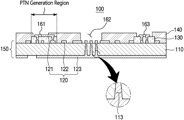
1. A multilayer circuit board, comprising:
a base layer;
a second pattern layer formed on one side of the base layer;
a first pattern layer formed on the second pattern layer;
an interlayer insulating layer formed between the first pattern layer and the second pattern layer, the interlayer insulating layer being partially formed on the second pattern layer so as to correspond to a region in which the first pattern layer is formed;
a protective layer that covers a part of the first pattern layer which is formed on the interlayer insulating layer and is located in the uppermost layer among a plurality of pattern layers, the protective layer is integrally formed on the second pattern layer and the interlayer insulating layer,
wherein
the protective layer covers the second pattern layer on which the interlayer insulating layer is not formed, a part of the interlayer insulating layer, and a part of the first pattern layer which is formed on the interlayer insulating layer, and
the number of pattern layers which is formed on both sides of the base layer is different; and
a third pattern layer formed on the other side of the base layer,
wherein the third pattern layer is electrically connected to the first pattern layer and the second pattern layer through a conduction hole formed in the base layer and a conduction hole formed in the interlayer insulating layer, and
wherein the first pattern layer is electrically connected to the second pattern layer through the conduction hole formed in the interlayer insulating layer.
|