| CPC H05K 1/0298 (2013.01) [H01L 21/4857 (2013.01); H01L 23/145 (2013.01); H01L 23/49822 (2013.01); H05K 1/115 (2013.01); H05K 3/4623 (2013.01); H01L 2224/16225 (2013.01); H05K 2203/1438 (2013.01)] | 18 Claims |

|
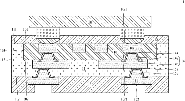
1. A semiconductor device package, comprising:
a first dielectric layer having a first surface;
a first interconnection layer disposed over the first surface of the first dielectric layer; and
a first metal layer partially disposed between the first surface of the first dielectric layer and the first interconnection layer;
a second dielectric layer covering the first surface and a lateral surface of the first dielectric layer; and
a first wiring layer disposed within the first dielectric layer, wherein the first wiring layer includes a first portion and a second portion separated from the first portion from a cross-sectional view, and a top surface of the first portion facing the second dielectric layer is free from being exposed by the first dielectric layer,
wherein a lateral end surface of the first metal layer is recessed with respect to a lateral end surface of the first interconnection layer by a first distance,
wherein the lateral surface of the first dielectric layer is recessed with respect to a lateral surface of the second dielectric layer by a second distance, and
wherein the first interconnection layer is disposed directly over the second portion, and a width of the second portion is greater than a width of the first portion.
|