| CPC H05K 1/0298 (2013.01) [H05K 1/11 (2013.01); H05K 2201/0212 (2013.01); H05K 2201/0394 (2013.01)] | 20 Claims |

|
1. A printed wiring board, comprising:
a first resin insulating layer;
a conductor layer formed on a surface of the first resin insulating layer; and
a second resin insulating layer formed on the surface of the first resin insulating layer such that the second resin insulating layer is covering the conductor layer,
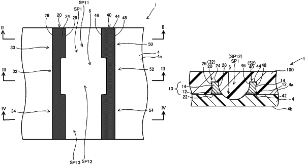
wherein the conductor layer includes a first conductor circuit and a second conductor circuit positioned adjacent to the first conductor circuit such that a space is formed between the first conductor circuit and the second conductor circuit, the first conductor circuit has a first side wall and a second side wall on an opposite side with respect to the first side wall, the second conductor circuit has a third side wall and a fourth side wall on an opposite side with respect to the third side wall such that the second side wall of the first conductor circuit faces the third side wall of the second conductor circuit, the first conductor circuit has a first portion, a second portion extending from the first portion, and a third portion extending from the second portion, the second conductor circuit has a fourth portion, a fifth portion extending from the fourth portion, and a sixth portion extending from the fifth portion such that the first portion of the first conductor circuit and the fourth portion of the second conductor circuit face each other, that the second portion of the first conductor circuit and the fifth portion of the second conductor circuit face each other, and that the third portion of the first conductor circuit and the sixth portion of the second conductor circuit face each other, the first conductor circuit is formed such that the second side wall of the second portion is recessed from the second side wall of the first portion and the second side wall of the third portion and that the space formed between the second portion of the first conductor circuit and the fifth portion of the second conductor circuit becomes larger, and the first resin insulating layer has a recess formed between the second portion of the first conductor circuit and the fifth portion of the second conductor circuit such that the second resin insulating layer is filling the space and the recess.
|