| CPC H05K 1/0274 (2013.01) [H05K 3/041 (2013.01); H05K 2201/10121 (2013.01); H05K 2201/10151 (2013.01)] | 24 Claims |

|
1. An optical package, comprising:
a Printed Circuit Board (PCB) comprising a plurality of cut-out sections;
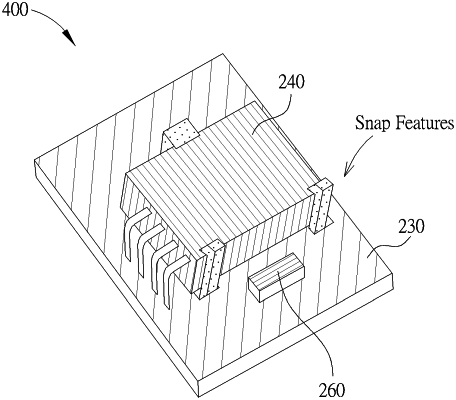
a lens, comprising a first plurality of protrusions corresponding respectively to the plurality of cut-out sections, wherein the first plurality of protrusions comprises three protrusions being snap features, a first protrusion of the first plurality of protrusions is formed on a first side of the lens, and a second protrusion of the first plurality of protrusions is formed on a second side of the lens opposite to the first side, and when the lens is placed under the PCB, the first plurality of protrusions will pass through the cut-out sections; and
a sensor for attaching on to the lens and the PCB;
wherein the snap features comprise inward-facing protrusions which attach to the top of the sensor.
|