| CPC H04N 13/271 (2018.05) [H04N 13/239 (2018.05); H04N 23/10 (2023.01); H04N 23/62 (2023.01); H04N 23/80 (2023.01); H04N 25/75 (2023.01); H04N 25/778 (2023.01); H04N 2013/0081 (2013.01)] | 20 Claims |

|
1. An image sensor comprising:
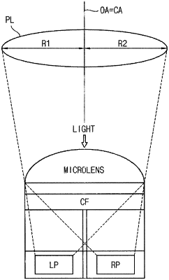
a pixel array including a plurality of pixels, each of the pixels including at least a first photoelectric conversion element and a second photoelectric conversion element, a microlens on the first and second photoelectric conversion elements;
an analog-to-digital conversion circuit configured to generate a pattern image data by performing an analog-to-digital conversion on a first analog signal output from each of the pixels in response to a pattern image located at a first distance from the image sensor and configured to generate an image data by performing an analog-to-digital conversion on a second analog signal output from each of the pixels in response to an object; and
a disparity calculation unit configured to calculate a disparity of the pattern image data,
wherein the disparity represents a difference between first pixel values of a first pattern image data and second pixel values of a second pattern image data, the first pattern image data being associated with the first photoelectric conversion element of the pattern image data and the second pattern image data being associated with the second photoelectric conversion element of the pattern image data.
|