| CPC H04B 1/005 (2013.01) [H01L 23/49822 (2013.01); H01Q 21/0025 (2013.01); H05K 1/0243 (2013.01)] | 19 Claims |

|
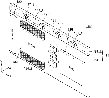
1. An antenna module comprising:
a multilayer board including an antenna configured to transmit and receive electromagnetic waves through a top surface of the multilayer board;
a radio frequency (RF) chip on a bottom surface of the multilayer board, the RF chip being connected to the antenna and configured to process an RF signal; and
a first active device array on the bottom surface of the multilayer board, the first active device array comprising a plurality of active devices, a first input pin and a first output pin,
wherein the first input pin and the first output pin are respectively connected to electrodes of a first active device of the plurality of active devices, and
the multilayer board comprises:
a first pattern for a first signal to be provided from the RF chip to the first input pin; and
a second pattern for a second signal to be provided from the first output pin to the RF chip.
|