| CPC H03M 1/46 (2013.01) [H03K 5/24 (2013.01)] | 19 Claims |

|
1. A comparator circuit comprising:
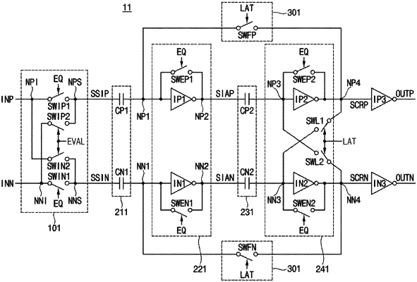
an input circuit configured to generate an amplified input signal through a sampling node by alternately selecting a positive input voltage and a negative input voltage during an equalizing period and a sampling period;
a first inverting amplification circuit configured to generate an intermediate amplified signal by performing an inversion and amplification operation based on the amplified input signal during the sampling period;
a second inverting amplification circuit configured to generate a comparison result signal by performing an inversion and amplification operation based on the intermediate amplified signal during the sampling period;
a first coupling circuit connected between the input circuit and an input node of the first inverting amplification circuit;
a second coupling circuit connected between an output node of the first inverting amplification circuit and an input node of the second inverting amplification circuit; and
a feedback circuit configured to amplify the input node of the first inverting amplification circuit with a rail-to-rail voltage corresponding to a power supply voltage or a ground voltage based on the comparison result signal during the sampling period,
wherein the first inverting amplification circuit includes:
a first inverter connected between the input node of the first inverting amplification circuit and the output node of the first inverting amplification circuit;
a first equalization switch connected in parallel with the first inverter between the input node of the first inverting amplification circuit and the output node of the first inverting amplification circuit and configured to be turned on based on an equalization signal having an activation period corresponding to the equalizing period; and
a second equalization switch connected in series with the first equalization switch between the input nod of the first inverting amplification circuit and the output node of the first inverting amplification circuit and configured to be turned on based on at least on of the equalization signal or a latch signal that is activated during the sampling period.
|