| CPC H03K 17/6871 (2013.01) [H03K 17/0812 (2013.01); H03K 17/0814 (2013.01)] | 12 Claims |

|
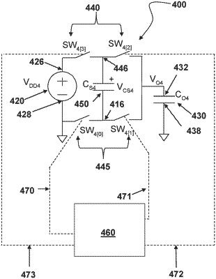
1. A capacitive element driver for driving a capacitive element between voltage levels, the capacitive element comprising an element having capacitive functionality and the voltage supplied to the capacitive element driver by a voltage source, the capacitive element driver comprising:
a plurality of switches having:
a first switch electrically connectable in series directly or indirectly between a first terminal of the voltage source and an input terminal of the capacitive element, and
a second switch electrically connectable in series directly or indirectly between a second terminal of the voltage source and the input terminal of the capacitive element; and
a plurality of non-dissipative elements arranged to store and transfer energy for driving the capacitive element between the voltage levels, wherein the plurality of non-dissipative elements is electrically connectable in parallel or in series directly or indirectly:
at a first end between the first terminal of the voltage source and the input terminal of the capacitive element, and
at a second end between the second terminal of the voltage source and the input terminal of the capacitive element;
wherein the plurality of switches is arranged to open or close in combinations in a sequence of switching stages to step-wise transfer the energy to the capacitive element, the sequence of switching stages further comprising a switching pattern having a voltage change portion arranged to cause a change in an output voltage of the capacitive element driver during application thereof on the capacitive element driver.
|