| CPC H03K 17/687 (2013.01) | 13 Claims |

|
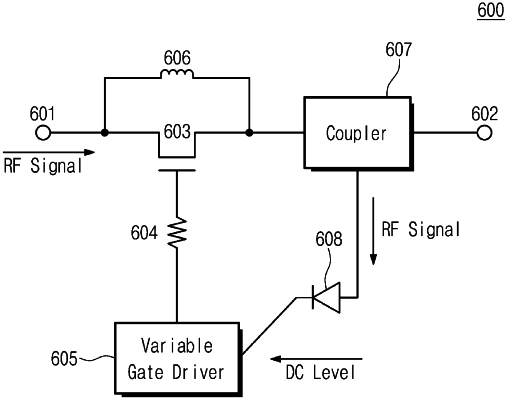
1. A switch circuit comprising:
at least one transistor including a first terminal connected to an input stage, a second terminal, and a gate terminal;
an inductor connected to the at least one transistor in parallel, between the input stage and an output stage;
a variable gate driver configured to apply a gate input voltage to the gate terminal;
at least one input resistor connected between the variable gate driver and the gate terminal;
a coupler connected between the output stage and the at least one transistor to extract a portion, which is transmitted to the output stage, of an RF signal applied to the input stage; and
a diode connected between the coupler and the variable gate driver to convert the extracted RF signal to be in a direct current (DC) level and to output the conversion result to the variable gate driver,
wherein the variable gate driver adjusts the gate input voltage to be in one of a first voltage level for turning on the at least one transistor and a second voltage level for turning off the at least one transistor, and
wherein the variable gate driver adjusts the gate input voltage based on the output DC level, when the at least one transistor is in a turn-off state.
|