| CPC H03K 17/08128 (2013.01) [H02H 9/04 (2013.01); H03K 17/08122 (2013.01)] | 20 Claims |

|
1. A switching circuit comprising:
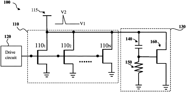
a main circuit comprising a plurality of first transistors and comprising a first node, a second node, and a third node, wherein the main circuit is operative in response to a control signal received by the first node, and the second node is configured to receive a supply voltage;
an auxiliary circuit electrically coupled to the second node of the main circuit and configured to provide surge protection for the main circuit, wherein the auxiliary circuit comprises a second transistor,
wherein a breakdown voltage of the second transistor is different than a breakdown voltage of each first transistor of the plurality of first transistors, and each first transistor of the plurality of first transistors comprises a first III-V based high-electron-mobility transistor (HEMT) and the second transistor comprises a second III-V based HEMT.
|