| CPC H03F 1/223 (2013.01) [H03F 1/301 (2013.01); H03F 1/56 (2013.01); H03F 3/193 (2013.01); H03F 3/195 (2013.01); H03F 3/213 (2013.01); H03F 3/245 (2013.01); H03F 2200/102 (2013.01); H03F 2200/105 (2013.01); H03F 2200/165 (2013.01); H03F 2200/18 (2013.01); H03F 2200/21 (2013.01); H03F 2200/222 (2013.01); H03F 2200/225 (2013.01); H03F 2200/243 (2013.01); H03F 2200/294 (2013.01); H03F 2200/297 (2013.01); H03F 2200/301 (2013.01); H03F 2200/306 (2013.01); H03F 2200/387 (2013.01); H03F 2200/391 (2013.01); H03F 2200/399 (2013.01); H03F 2200/42 (2013.01); H03F 2200/451 (2013.01); H03F 2200/48 (2013.01); H03F 2200/489 (2013.01); H03F 2200/492 (2013.01); H03F 2200/498 (2013.01); H03F 2200/555 (2013.01); H03F 2200/61 (2013.01); H03F 2200/78 (2013.01)] | 20 Claims |

|
1. A method for biasing the final stages of a cascode amplifier, including:
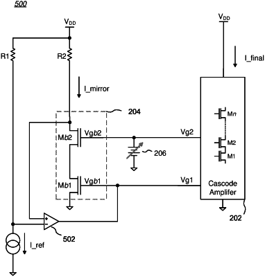
(a) providing a cascode amplifier having at least two serially connected field effect transistor (FET) stages, each FET stage having a gate, a drain, and a source, the bottom FET stage having an input configured to be coupled to an RF input signal to be amplified, and the top FET stage of the cascode amplifier having an output for providing an amplified RF input signal;
(b) providing a cascode reference circuit having at least two serially connected FET stages, each FET having a gate, a drain, and a source, the gates of the bottom two FET stages of the cascode reference circuit being coupled to the corresponding gates of the bottom two FET stages of the cascode amplifier, for biasing the cascode amplifier to output a final current approximately equal to a multiple of a mirror current in the cascode reference circuit; and
(c) providing an op-amp having a first and a second input and an output, the first input being coupled between a voltage source through a first resistor and a reference current source, the second input being coupled between the voltage source through a second resistor and the drain of the top FET stage of the cascode reference circuit, the output being coupled to the respective gates of the bottom FET stages of the cascode reference circuit and the cascode amplifier, wherein the op-amp is responsive to differences between its first and second inputs and outputs an adjustment gate bias voltage applied to the respective gates of the bottom FET stage of the cascode amplifier and of the cascode reference circuit that forces the mirror current in the cascode reference circuit to be approximately equal to a selected current value.
|