| CPC H01S 5/3402 (2013.01) [H01S 5/3407 (2013.01); H01S 5/34313 (2013.01); H01S 5/34366 (2013.01); H01S 2304/02 (2013.01)] | 6 Claims |

|
1. A quantum cascade laser, comprising:
a plurality of light-emitting quantum well layers configured to emit infrared laser light by using an intersubband transition; and
a plurality of injection quantum well layers configured to relax carrier energy,
the light-emitting quantum well layers and the injection quantum well layers being stacked alternately, the injection quantum well layers relaxing the energy of carriers injected from the light-emitting quantum well layers, respectively,
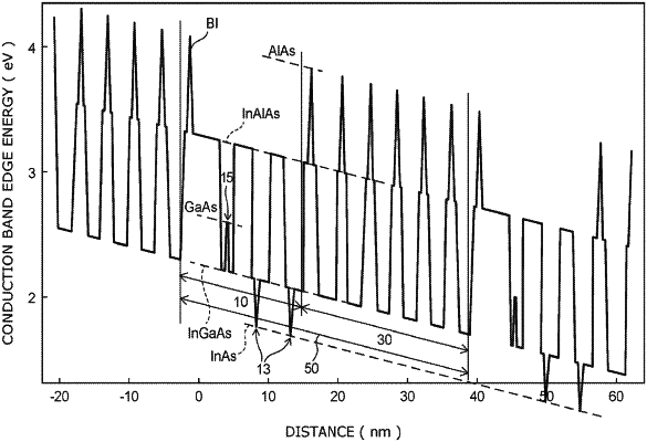
the light-emitting quantum well layers and the injection quantum well layers including barrier layers and well layers, the barrier layers including a first ternary compound semiconductor represented by a compositional formula of In0.36Al0.64As, the well layers including a second ternary compound semiconductor represented by a compositional formula of In0.67Ga0.33As, at least one of the barrier layers of the injection quantum well layers including a first region, a binary compound semiconductor thin film and a second region, the binary compound semiconductor thin film being provided between the first and second regions, the first and second regions being of the first ternary compound semiconductor,
the binary compound semiconductor thin film including a binary compound of AlAs,
wherein the binary compound semiconductor thin film has a film thickness equal to or less than a thickness of double atomic-monolayers including Al atoms and As atoms,
a conduction band edge energy of the binary compound semiconductor thin film of the barrier layers of the injection quantum well layers is higher than a conduction band edge energy of the barrier layers of the light-emitting quantum well layers, and
wherein the light emitting quantum well layers includes a well layer that includes another binary compound semiconductor thin layer of GaAs.
|